**MIP** stands for **Mini LED in Package**. It is an advanced packaging technology for LED displays, representing a significant evolution toward next-generation fine-pitch and Micro LED displays. It is not a type of display panel (like LCD or OLED) but rather a **manufacturing and packaging process** for the tiny LEDs that make up the screen.
At its core, MIP is a **hybrid approach** that combines the best features of two existing technologies: **SMD** and **COB**.
**Core Concept: The MIP Process**
The MIP process involves two key stages:
1.Micro-Unit Pre-Packaging:** Individual, microscopic red, green, and blue LED chips are first **pre-packaged** into standalone, functional pixel units. Each of these micro-units is a complete, miniature LED package with its own electrical contacts and, often, a tiny reflective cup for better light control.
2. Surface-Mount Assembly & Mass Transfer: These standardized, robust MIP "micro-packages" are then placed onto the display driver board using highly precise, high-speed surface-mount technology (SMT) machines—similar to how traditional SMD LEDs are placed but at a much smaller scale.
3.Encapsulation: Finally, the entire module is covered with a protective epoxy or resin layer (similar to COB), providing environmental sealing and mechanical strength.
Key Advantages of MIP Technology
1. High Reliability & Ruggedness: Like COB, the final protective layer makes the screen highly resistant to physical impact, moisture, and dust. This makes it ideal for high-touch environments like control rooms and public installations.
2.Superior Image Quality: The pre-packaged design allows for excellent black surface" uniformity (all non-emitting areas appear consistently dark). This results in higher contrast ratios, better color saturation, and reduced glare compared to traditional SMD.
3. Excellent Repairability: This is a major advantage over COB. If a single pixel fails, the individual MIP package can be precisely removed and replaced using repair equipment, solving COB's biggest drawback of being nearly impossible to repair at the chip level.
4.Manufacturing Efficiency & Yield: It leverages well-established, high-yield SMT processes for placement. Pre-testing the MIP packages before assembly also improves overall production yield and cost control, especially at very small pixel pitches (below P1.0mm).
5. Bridge to Micro LED: MIP is widely seen as the most viable and scalable pathway to mass-producing true Micro LED displays(where chip sizes are below 100µm). It solves the massive technical challenge of transferring and assembling billions of bare, microscopic chips.
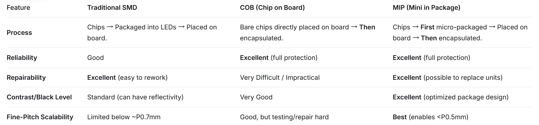
Comparison with SMD and COB
Primary Applications
MIP technology is used in high-end professional displays where image quality, longevity, and reliability are critical:
* Broadcast Studios & Virtual Production Volumes (The "LED Wall" for film/TV)
* Corporate Boardrooms & High-End Conference Rooms
* Command and Control Centers
* Premium Commercial Signage (Retail, Luxury)
* Future: High-end home cinema and large-format TVs.
Summary
In short, an **MIP LED screen** is a display built using a next-generation packaging method where LEDs are **first miniaturized and packaged as individual pixel units, then mass-assembled onto a board, and finally sealed for protection.** It successfully merges the **repeatability and manufacturing efficiency of SMD** with the **superior ruggedness and image performance of COB**, positioning itself as the leading technology to enable the future of ultra-fine-pitch and Micro LED displays.

Name: Jerry
Mobile:+8615915361141
Tel:86-0755-82599892
Whatsapp:8615818291783
Email:info@conwinled.com
Add:Room 313-315, Building A, Sanlian Industrial Zone, Shiyan Street ,Shenzhen, China